High-Throughput Materials Discovery for Metal Halide Perovskite Light Emitters

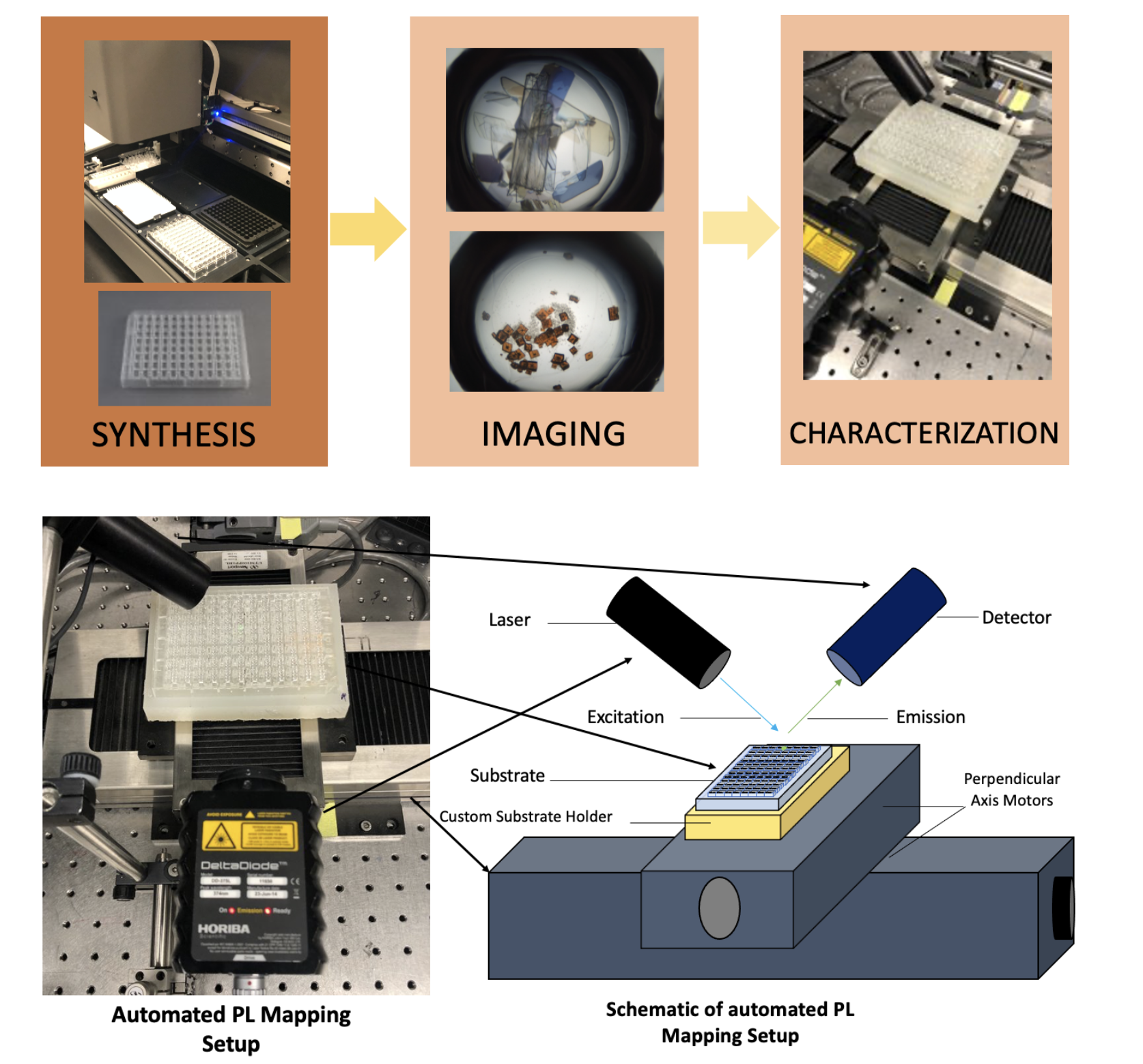
In the past decade alone, thin-film metal-halide perovskite (MHP) solar cell power conversion efficiency (PCE) has increased from 3.8% to 25.5%. MHPs have small exciton binding energy, balanced electron, and hole mobilities and long exciton diffusion lengths. The high PCE achieved in solar cells has encouraged research into MHPs for use in LEDs and they have demonstrated high photoluminescence quantum yields (PLQY) and narrow peaks. This project will use an HTE approach and ML models to understand the origins of previous low emission efficiencies and large emission linewidths to inform research towards bright narrowband emitters. Single crystal fabrication benchtop methos require ~5 days to grow a single crystal and another day to characterize them. This means that a full-time experimental (FTE) researcher can only explore a few materials and conduct 5-10 experiments on each material over the course of a week. We have been able to accelerate this to up to 5000 experiments/week across 20 materials. An autonomous PL measuring setup was built to gather spectral emission in high-throughput to screen MHP consisting of two perpendicular motors, an excitation source (375 nm diode laser) and a detector (Ocean Optics 2000+ Spectrometer) in the configuration. The motors are programmed to move the substrate in a snake-like pattern, allowing the laser to excite each drop while the detector measures the spectral PL response of the crystal in the drop. The resulting spectra has been compiled into a dataset with the experimental parameters used to grow each crystal. This data was compiled into a dataset and used to train ML models to identify groups of materials that may share desired properties such as brightness, peak position and linewidth. 17 new materials were discovered using this method and published for further exploration by the perovskite community (ACS Cent. Sci. 2022, 8, 5, 571–580).
Machine-Learning Assisted Hole Transport Material Discovery for Quantum Dot LEDs

Thin-film LEDs, such as quantum dot LEDs (QD LEDs), require additional transport layers to aid in charge injection and extraction from the electrodes into the active material. The typical device architecture for a thin-film LED involves a pair of electrodes, a hole and electron transfer layer (HTLs and ETLs) and a light-emitting active layer sandwiched between the two. The transport layers inject charge carriers from the electrodes into the active material where they recombine radiatively and emit light. These transport layers are typically organic transport layers tend to be chemically unstable, along with being sensitive to moisture, temperature, and other atmospheric onditions. Inorganic alternatives to HTL materials are needed to produce the next generation of stable and bright QD LEDs with high emission efficiency.

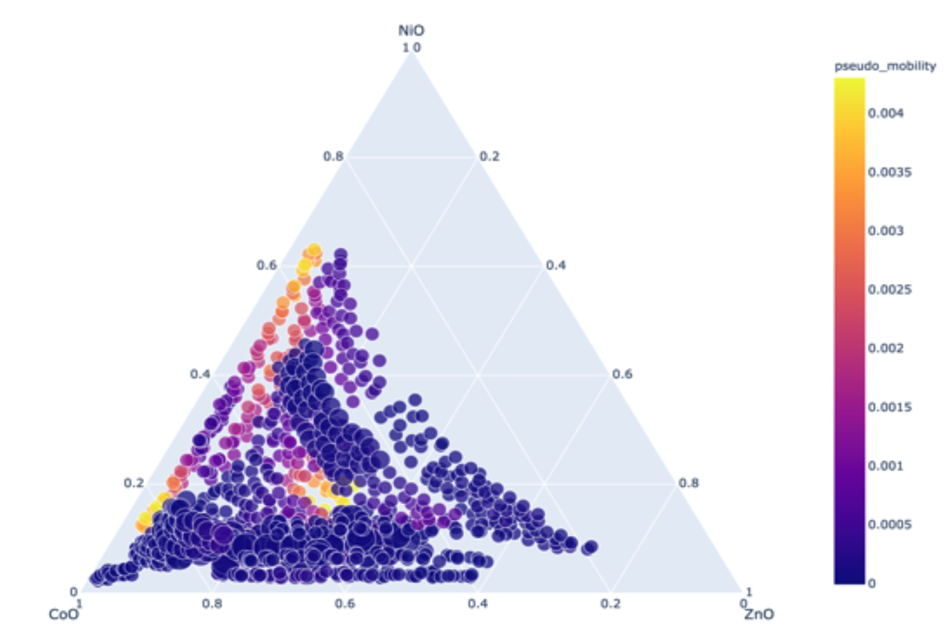
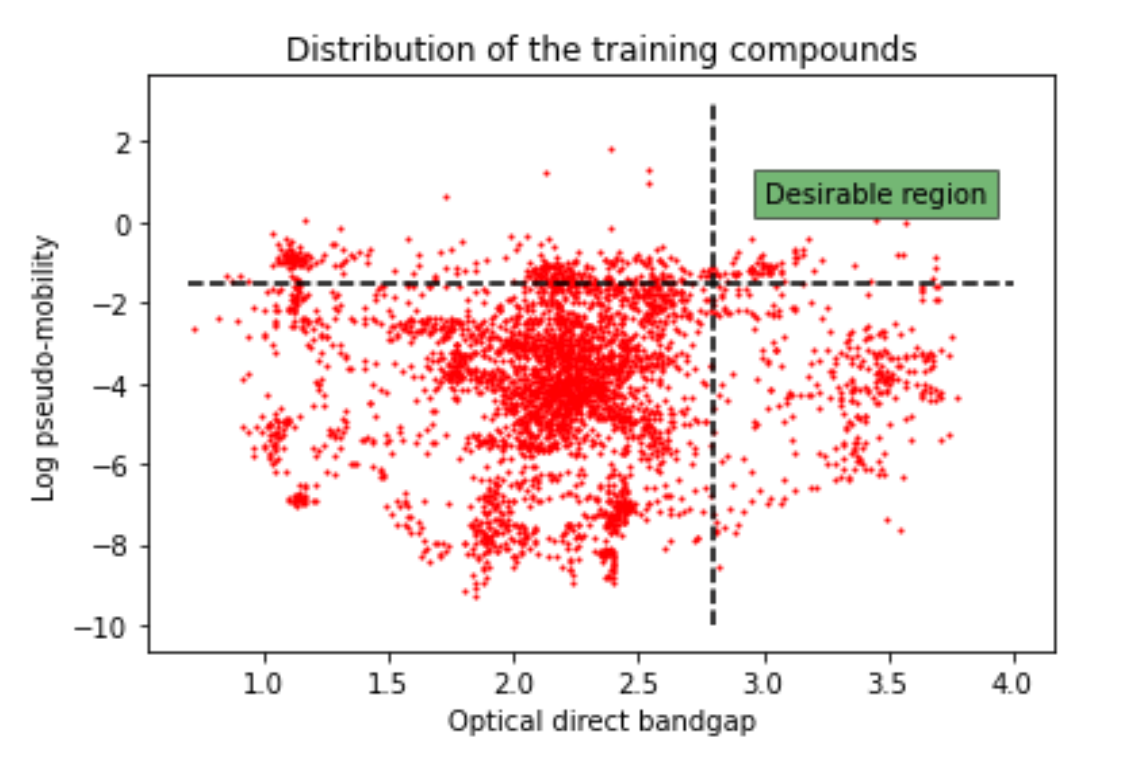
This first project leverages an existing dataset produced by the National Renewable Energy Laboratory (NREL). The High Throughput Experimental Materials Database (HTEM DB) database contains spatially resolved characterization data for inorganic thin films deposited using combinatorial physical vapor deposition (PVD) methods. The database has been used for high throughput exploration of electronic and energy materials, but this is the first report to use it for mobility studies. Using this database, I train three ML models to predict key optical and electronic properties for inorganic metal compounds such as conductivity, mobility, and bandgap. The model predicts absorption spectra for the first time using just the stoichiometric representation of a proposed compound. This negates the need for multiple device fabrication and characterization, accelerating the optimization of a ternary metal oxide by 5x-10x. The model also performs 1000x faster than using DFT to predict absorption profiles, and the bandgaps derived from our profiles have a 3x lower MAE. To validate the methodology, I estimate a proxy for mobility using conductivity and absorption. Finally, I leverage the model to optimize the conductivity of sputtered Cu- doped NiOx and fabricate samples experimentally for confirmation. I observe a 2x improvement in conductivity over pristine sputtered NiOx.
\[\\[1in]\] \[\\[1in]\]
Investigating the Origin of Phase Transition During the Crystallization of Rb-substituted Wide-Bandgap Perovskite Thin-Films

CsPbX3 was the first perovskite ever studied for optoelectronics in 1958 when researchers discovered that Cl- or Br-based CsPbX3 resulted in colored crystals that demonstrated a photoconductive response. However, it took over half a century for these inorganic perovskites to result in functioning PV devices in 2015. This optoelectronic property has since been exploited for a range of electronic devices but these perovskites still suffer from instability. Phase segregation occurs as ions migrate in the presence of vacancies, degrading the PCE and stability of the perovskite layer. Passivation with alkali metal cations has been employed with great success. Rb+ incorporated organic-inorganic perovskites have been observed to improve crystallization kinetics and hence the overall thin-film quality. However, little is understood of the mechanism through which Rb+ influences the crystallization of the thin film.
The use of synchrotron-based grazing incident wide angle X-ray scattering (GIWAXS) has thus become an indispensable tool for investigating and comprehending the structure of perovskite thin films. The rapid and extensive adoption of GIWAXS experiments—both in-situ and ex-situ—has generated large amounts of data that are typically thoroughly analyzed by hand.
In this work, I use a custom-built in-situ spin-coating and annealing setup that integrates with Brockhouse XRD and Scattering Sector Low Energy Wiggler (BXDS-WLE) beamline of the Canadian Light Source. I study the wide-bandgap perovskite composition Cs1−xRbxPbI1.75Br1.25 (x= 0.05-0.20) and gather time-dependent dataset of images to track crystallization over the spin-coating and annealing process. We conclude that a threshold amount of Rb negates the degradation brought about by Br incorporation. We observe that x=0.15 suggests the creation of a stable active perovskite until prolonged annealing results in degradation to the delta phase. Lower or larger amounts of Rb do not translate into improved stability or device performance. The dataset comprised of ~10,000 GIWAXS 2D diffraction images are integrated into 1D linecuts, normalized, and were subsequently used to extrapolate how varying the A-site cation will affect a given perovskite composition without having to conduct lengthy in-situ experiments, reducing the dependance on synchrotron beamtime.
Publications:
- Sequential Co-Passivation in InAs Colloidal Quantum Dot Solids Enables Efficient Near-Infrared Photodetectors
- High-Throughput Evaluation of Emission and Structure in Reduced-Dimensional Perovskites
- Dipole Engineering through the Orientation of Interface Molecules for Efficient InP Quantum Dot Light-Emitting Diodes
- Triplet State Formation in Photovoltaic Blends of DPP-Type Copolymers and PC71BM